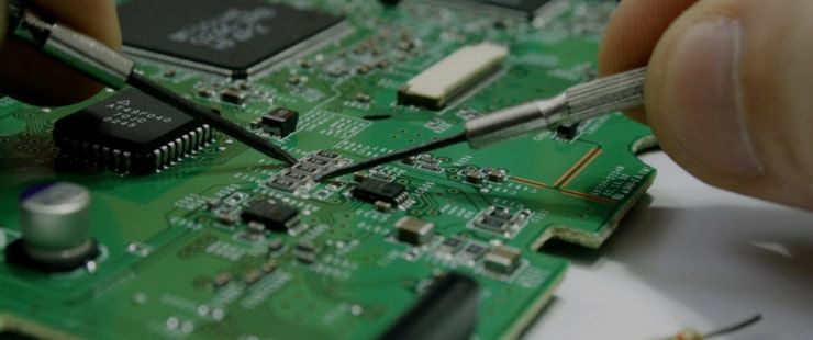
 To show circuit functionality and be readable PCB assembly layout designers in the past worked from schematics that usually drawn in a meaningful way. For instance, angled wires pointing to each other indicates by the cross-page connection. The PCB designers logically made the physical parts placement follow the schematics, and the components that formed functional groupings tended to remain co-located. Usually, the schematics can be read and understood by others, which includes those schematics that were used later to perform troubleshooting, deduce circuit operation, and repair. However, it was relatively easy to recreate a schema from such a PCB assembly. More then, CAE and CAD came along. Into an electronic Etch A Sketch capture tool the art of schematic drawing became debased, whose primary purpose was to create a netlist. So, to complete the planting of the copper traces the PCB designer could use a "rat's nest" on-screen display. In the digitized dumbing-down, any semblance of analog rules or communication between the design engineer and the PCB layout designer was lost. Based on actual PCB placement and package pin-outs, reverse analysis is a two-pass effort requiring an initial physical schematic. Re-drawing the captured circuits in a logical and comprehensible fashion the series of the functional schematic followed. Moreover, the PCB assemblies’ representation is the real schematic. As on the PCB assembly, components drawn in the same orientation and with GDS or EBC physical pins transistors shown in their representative packages. Arranged in the same way relay switches are sown with their terminals as they appear from the top. With the display of functional names and internal logic elements, ICs drawn in their packages. Relating components to a later functional schematic strongly varies on the physical schema, as most of the times a PCB assembly does not have reference designators in the silkscreen. It is impossible to figure out what is going on electrically. However, the result is a very readable and understandable depiction once this has been re-drawn into a meaningful functional schematic. Temporarily color-coding the nets on the physical drawing make the transfer to the technical drawing less prone to error and when dragged around for readability, flexible wires follow the components. Unfortunately, when an element is rotated or flipped, TinyCAD does not keep wires connected. For instance, you have your physical schematic drawn out on a single page, with everything scrunched up close together, impossible to make any sense of the actual electrical functions and long runs of closely spaced wires. Setting its color to bright purple, width to 25 and apply to the entire net with just a click on a fence, suddenly that net jumps off the page at you. Additionally, any net throughout the page with the same name attached will also brighten into visibility. Hence, an individual should have some form of revision control to keep track of the latest updated drawing when others need access to it. So is your PCB assembly no longer manufactured or you need any replacements or capacity additions? Lost your drawings or schematics from corrupted files? Reverse engineer is the best solution. Reverse engineering of PCB’s is one of PCC specialties and our PCB and PCA knowledge with long years of manufacturing experience, has enabled us to provide optimum PCB Reverse Engineering Services. With proficiency and understanding of PCB Reverse Engineering Process, PCC has a dedicated team of engineers following IPC design specifications and work on simple to the most complex PCB/PCA projects.
46 Comments
 The electronics manufacturing spectrum has never been in short of skilled professionals building perfect circuit boards no matter how small and complicated they may be. And it is a universal fact that 100 per cent perfection is not possibly achievable. For large production runs, a small number of defects do not pose threat as such. However, when the demand is for a customized circuit board or a unique prototype, the cost to recreate it would be huge. And proceeding with the defective piece would be disastrous. In such cases, PCB repair and rework is one of the best options to save an investment from being a failure. PCB repair services in fact can save money and resources in cases of failure.
Introducing Reverse Engineering There are several reasons to carry out reverse engineering services of a Printed Circuit Board (PCB). One amongst them is that industries invest huge capital on machine systems. Many a times, these expensive machines can go down simply because of one component in a PCB. It makes logical sense that when a company invests in an expensive machine system, it would be imperative for it to utilize it for many years. In many cases, it has been observed that an original equipment manufacturer (OEM) goes out of business while the machine system developed by them is still running. Now a machine on which so much of investment was made is left without the facility for support and an inability to get it repaired. In the electronics manufacturing sphere, it has been observed that in a time span of 15 to 30 years after a machine was installed, only one or two components or PCBs become defective requiring replacement or repair. Reverse Engineering: A Systematic Process The process of reverse engineering may include the following: 1. Perceiving specifications and engineering sketches This is done to identify and analyze the components of the machine and their relationship with one another. 2. Electronic analysis of the system This constitutes analyzing each component’s electronic aspects like, electromagnetic interference, radio frequency, control loops, and communication and contacts between parts. 3. Obsolescence analysis of components This allows companies to make room for spare parts and support for components such as circuit boards that have become obsolete years ago. 4. Component Information analysis Information is extracted when components and their interrelationships are thoroughly studied. The diagrammatic representation of the information discovered proves to be of great help in the process. 5. Process variation of the reverse engineered system The diagrammatic representation facilitates creating a physical version by reassembling the different parts and components. Reverse Engineering vs Repair & Rework Reverse Engineering when compared to repair and rework is quite a different approach altogether. They, however, serve the same purpose. And that is making the components or PCBs or the whole machine systems free from defects. Reverse Engineering comes into play when repair, rework, or modification for a machine system becomes difficult or impossible. For instance, when a machine system whose OEM is out of business fails due to a defect in one or two components, it becomes necessary to carry out reverse engineering. Moreover, reverse engineering also facilitates research and development of electronics. So, both repair and rework, and reverse engineering have their own significance in the electronics manufacturing industry. Rather than having a comparison between the two, it is better to look at both as systematic processes being parts of a diverse discipline. |
 RSS Feed
