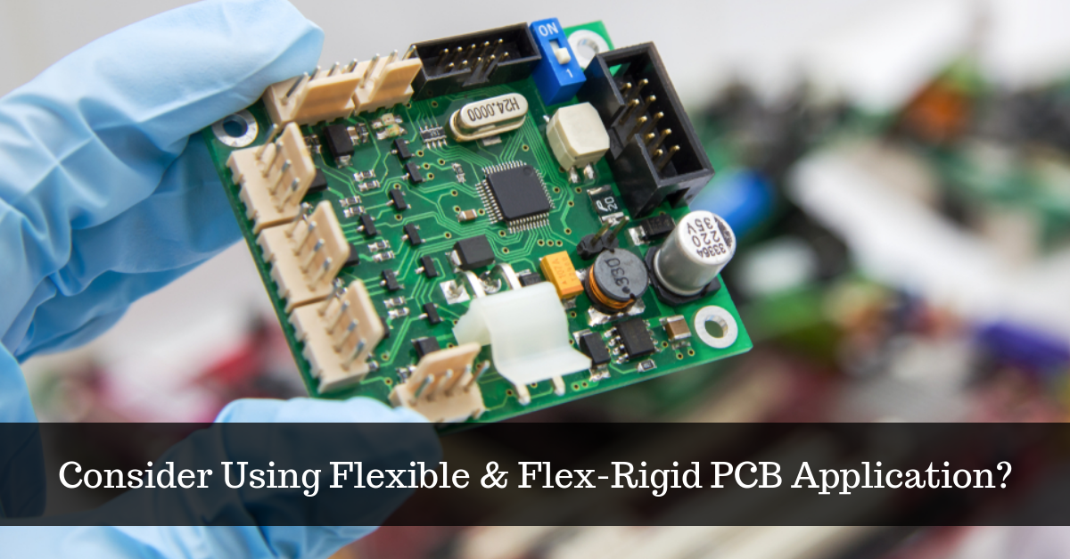
 Each assembles, and devices begin with the core component, which is Printed Circuit Boards (PCBs). Are you considering the use of flexible and flex-rigid PCBs in an upcoming device, product, or prototype? It mainly depends on which type of PCB assembly you choose for your application. Flexible and Flex-Rigid Printed Circuit Boards are the two significant types of circuitry and boards used in industrial and large-scale manufacturing sites. They vary from traditional and rigid Printed Circuit Boards.
With the combination of flexible and rigid materials as well as technologies, these PCB assembly boards get designed. And these flexible printed circuit boards are rolled with copper and similar materials, providing ample flexibility and winding resistance. On the other hand, flex-rigid PCBs are built using a combination of two technologies, along with both flexible and rigid areas. Let us have an in-depth understanding of Flexible Printed Circuit Boards and Flex-Rigid Printed Circuit Boards. Flexible PCBs Assembly The term flexible printed circuit boards reflected the word flexible for multiple reasons. However, their circuitry can be designed to match up with the electronic device or core product. Further, to create a product, or almost casing the board it is not a compulsion for the manufactures; instead, they can adapt it to fit an existing design. As a result, it is beneficial while creating components or hardware that feature a conventional design. For instance, if you are apprehensive with the total weight, portability, and resilience of a specific device, traditional boards may be out of the question. At times, these flexible boards must get adapted to products limitations. Traditional PCB Assembly is also rolled out, apart from the materials used are much more substantial and more rigid. Flexible PCB Pros and Cons: • Reliability is excellent due to the removal of mechanical connectors • Higher cost than rigid or flex-rigid • Fair temperature resistance • Flexible and pliable • Can accommodate any design • Better for rapid movement and high-stress conditions Flex-Rigid PCB Assembly The combination of flexible and inflexible circuitry areas derive the name of flex-rigid PCBs. Moreover, similar to most of the printed circuit boards, they have multiple layers yet more than conventional designs. Further, depending on the product needs, these additional conductive layers are drafted with rigid or flexible insulation. It barely matters, about the number of outer layers on the board, as they usually contain imperilled pads or covers for safety. Moreover, for the primary rigid layer, conductors are deployed. On the other hand, flexible plated through-holes are used for any supplementary layers, both flexible and inflexible. As per the research study, few projects demand traditional rigid technologies and designs. Whereas others have their limitations, preventing manufacturers from adopting these more comprehensive and less flexible boards. Illustration: If designed with standard boards, mobile and portable devices would suffer, as there are too many moving parts and components performing poorly when subjected to certain conditions. It is a must that mobile devices require to be portable, lightweight, and able to tolerate any seasonal conditions. Pros and Cons of Flex-Rigid PCB • Reliability acts as an outstanding, due to less requirement for solder joints • Lower cost compared to flexible boards • Works best at temperature resistance • Ideal for modest to somewhat higher than normal movement and stress • More flexible and pliable in comparison to conventional boards • Long-term reliability thanks to fewer interconnects and components • Requires minimal maintenance Hence, these two printed circuit boards assembly applications - Flexible and Flex-Rigid PCBs make them well suited for different applications with their unique capabilities. With over a decades, PCC specializes in rapid PCB assembly & system manufacturing services. We provide PCB Assembly Services for low and medium volume, high mix products, to varied customer markets globally. Our CCA, circuit card assembly lines are versatile for various sizes and substrates types (FR4, Rogers, copper, duroid, ceramic, metalcore aluminum, CEM 1, and CEM 3). From Design of Manufacturing (DFM), material sourcing, to testing, we provide in-house, end to end support services to deliver quick turnkey PCB assemblies and consignments.
24 Comments
 Often have we heard about reverse engineering with mechanical engineering, but how does this deploy in electronics and why? To understand it, let us first understand what is Reverse Engineering?
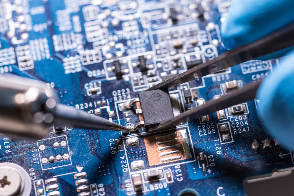
Reverse Engineering The term ‘reverse engineering’ frequently used in an electronic product environment to replicate a product. The examination of a competitor’s design has become commonplace for companies to use some aspects of the reverse engineering process. Occasionally using reverse engineering techniques, the base will even clone a competitor’s design, extracting a schematic from a Printed Circuit Board being the keen-witted of all the reverse engineering tasks. However, the reality is that there can be a genuine demand for this engineering on your products because some or all of the data package used to create the original product has gone missing/ no longer stored — an all too common problem. Why companies are looking to reverse engineer a PCB? Once a company has started this process, aside from replicating a lost schematic, they then have the choice to vary from the product that has to reproduce. Component obsolescence issues can be one of the reasons behind this. However, new agency standards are needed to adhere or a modified form factor. These can be the general product evolutions both by preference or requirement. But we have to sharpen our self-first on the missing element and data that is causing us to have a reverse engineer. The question that now occurs in our mind is, from where do we start, as the scenarios are many, with missing schematics, bill of materials, and Gerber or PCB assembly data. Here at PCC, we can extract and replace virtually any piece of missing data working from a PCB assembly or any accompanying electronic data, with the help of our dedicated team of engineers, who have complete knowledge and understanding of PCB Reverse Engineering Process. Our engineering expert team follow IPC design specifications and will work on simple to the most complex PCB/PCA projects. PCC’s PCB Reverse Engineering Services assist you with obsolete PCB replacement or repair, change PCB layout, reverse elaborate multilayer cards, recompile microcontroller program and edit source code logic, re-engineer an old PCB design to current standards, using new components, re-engineering for cost reduction/obsolescence Embedded processor/DSP based designs updating, reproduce lost or missing PCB or mechanical manufacturing files, and create new reference designs. With 27+ years of experience, PCC has been serving global clients, providing unique project-based re-engineering and copying of your printed circuit boards (PCBs). Our comprehensive services include PCB Clone (copy of the schematics and BOM), PCB Prototype (produce prototypes for market evaluation or testing) and PCB assembly production (Mass production of PCB or Assembly). 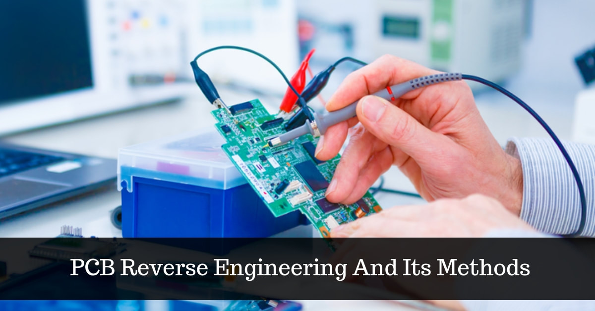 When a domestic electronic comes in need of repairs and servicing but its circuit diagram is unavailable, or the PCB has taken out of circulation, there might be a fatiguing task ahead as far as the repairs are concerned. The only way to re-create the PCB electronic circuit diagram in such cases is to reverse engineer the PCB electronic.
PCB reverse engineering is the process of replicating the functionalities and specifications of a PCB electronic by dissecting and analyzing the PCB electronic with or without the use of the manufacturing documents. It’s a tedious task, as it requires you to progress from a point where you have minimal information about a product to a point where you can roll out the production of the said electronic board. With PCB reverse engineering, you can re-position and replace old components, enhance various functionalities, and analyze and reinforce security in a PCB electronic. Methods of PCB Reverse Engineering Usually, PCB reverse engineering revolves around the following ways: On Your Image Editing Software, Prep Pictures of the Printed Circuit Board First, take the most detailed pictures of both sides of the Printed circuit board assembly or scan it by placing the bottom side of the board on the scanner. However, due to the obstructing height of the components, most of the scanners are unable to capture the top layer. Following this, import the picture to an open window of your favorite editing program. Here we are using Adobe Fireworks. Once the files are imported, organize the image in separated layers, and using the Polygon Lasso tool, crop all sides of the board from all pictures. Next, in the correct positions place the image using the Rotation CW/CCW and Flip Horizontal/ Vertical options. To ensure that all the sides of the images properly aligned with each other, use the zoom/magnifier tool. However, it is vital for all the pictures to be correctly aligned. Reduce the top layer’s opacity to around 50 – 75 percent to make it more transparent. Combine the Images There are copious ways to coalesce images, to have a range of options available for you to choose the one that works best for you, depending on your board color, illumination, and other optical factors. Screen Amalgam: Drag the bottom side up towards the component side to use screen amalgam. Then, to dim the copper layer, set the bar in the Brightness/Contrast filter to - 50. Next, highlight the copper layer and then choose blend mode on the Screen/Interpolation or Average (set to 80). Luminosity Blend: Drag the bottom side up towards the component side, and use the Levels filters to increase the contrast of the copper layer. Following, highlight the copper layer and select blend mode in Luminosity and set to 50. Brush and Threshold the Picture Drag the bottom side upwards toward the component side, and highlight the copper area by drawing a network of lines that connect the solder pads and holes using Brush. It is advisable to select colors that do not match with the solder mask. Later, extract only the solid color using the levels filter or threshold filter, and move the left pin across to the right. Ensuring this, adjust the Hue/saturation filter and select your preferred track color, rotating the Hue. Next, choose the blend in additive mode by highlighting the copper layer, and adjust the track’s intensity by setting the opacity to around 70. The last and final step is to record the values and replicate the benefits on CAD software. Hence, PCB engineering is a tedious task that requires not only expert technical knowledge but also a lot of strength of character. At PCC, we have a dedicated team of engineers with proficiency and understanding of PCB Reverse Engineering Process. Our engineering expert team follow IPC design specifications and will work on simple to the most complex PCB/PCA projects. Our PCB and PCA knowledge with extensive years of manufacturing experience has enabled us to provide optimum PCB Reverse Engineering Services.  When it comes to the electronic manufacturing process, launching of new products successfully into the market involves phases with both challenges and complexities each of which closely associated with another. However, it is common to see that great idea fails to smoothly convert into a product just due to insufficient focus on one or some steps, which primarily makes sense when, for instance, product concept fails to be fully validated or even becomes degrading, or an approved product has not optimized in terms of cost-effective electronics manufacturing and assembly. With an exciting idea, New Product Introduction (NPI Services) starts by transforming into a final electronic product after going through delicate design, automated manufacturing, and assembly, rigorous inspection, and testing.
New Product Introduction (NPI) Well, nothing is more complicated than getting high-quality products to market fast. Distributed teams using different tools and sharing information with external supplier partner’s means that it is easy to slip up and work on the wrong design. The need to innovate and get your products first to market says that you need a way to keep the entire product team on the same page. As team move from early concepts to prototypes to production, New Product Introduction (NPI) processes affect numerous teams, product lines, and supply chain partners that required to develop and ship products. A good NPI process is the foundation for any launch of the successful outcome and helps increase sales, customer satisfaction, as well as revenue growth. Critical Elements of a New Product Introduction
PCC provides complete end-to-end NPI service, starting from product analysis, prototyping, testing and verification against the specifications, to quality compliance and finally a seamless transition to the production phase. The key activities include:
>Feedback for improvements
>Availability analysis >Feedback for improvements
> FP (Flying probe) test > ICT(In-circuit test) > Functional tests > Boundary scans > Compliance tests > PFMEA (Process Failure Modes and Effects Analysis) Apart from NPI, PCC provides reliable electronic prototype development services, for both turnkey and consigned prototypes. Our rapid prototyping services help the client with faster design cycles and production capabilities. Our clients benefit with lower product development cost and market them faster by involving us in the early stages of production. We deliver turnkey PCB assemblies within two business working days. Our quote turnaround time is less than 48 hours. PCC has 27+ years of experience in delivering high quality, quick turn PCBA prototyping, and NPI services. Our team is highly skilled and regularly trained by IPC certified trainers. Our soundtrack record and consistent performance have earned us the recognition as the best electronic prototype development team in the USA. Our Prototyping and NPI Services are highly flexible to meet any Electronic Manufacturing Services (EMS ) need or requirement. We have the right team and equipment that you can trust. 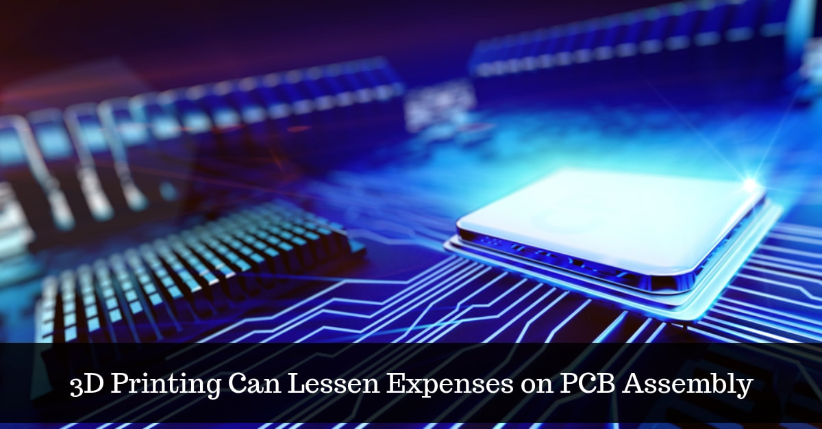 Working in a technology field is tricky like a puzzle, if one piece remains out of place, the picture looks incomplete. It is imperative that the tools of the trade made from quality standards. However, it can prove to be expensive while doing the same. Fortunately, in the works which drastically reduces the cost exists a new method to make quality tools which include prototype PCB Assembly.
With an ever-expanding technology, it has alarmed a matter of balancing out new technology with a modest means. Therefore, it is essential to find different ways to make the parts quicker and cheaper to stay updated in the industry, at which prototype PCBs can sustain its uses. Nowadays, 3D printing has become a massive industry, and it is apparent to see why due to vast varieties of items able to be printed undeviatingly of the computer at a fraction, which would usually cost. In France, one of the electronic industry had currently reported having commenced incorporating 3D printing across its manufacturing systems. Now, what does this mean for prototype PCB Assembly? In 2013 around USD 43.4 billion in revenue had accumulated from the printed circuit board and electronic component manufacturing in the United States. This medium means the cost-effective ways of printing out prototype circuit boards which can only increase the revenue gained substantially. PCB assembly will turn out to be the simplest way, with the use of this technology. As the delicate and pinpoint accuracy of needing to get every tiny puzzle piece of a printed circuit board down it will save time and can be done with a precision machine. This medium will not only create functioning prototype printed circuit boards more efficiently but will also assemble at an astonishingly faster rate. In addition to that, the savings made from transitioning to 3D printing will be astronomical. It saves time to assemble, which in itself saves money. And the material used to create circuit boards can be better utilized in a machine, thus preventing waste. While the material used to create the prototype circuit boards will remain the same, and therefore not provide lower costs, the time saved mass producing them is enough to create a vast difference in savings. In the world we live in, we are always looking to produce things faster, better and cheaper than what we created yesterday. The endless amounts of uses a simple 3D printer has on countless industries make it hard not to want to go out and grab one right away. PCC has two decades plus of experience in providing high quality, Electronic Manufacturing Services on time to varied groups of OEMs. From extensive printed circuit board assemblies to complex box-build/system integrations, we ensure flawless product delivery, with the desired degree of lead time and order flexibility. We have specializes in rapid PCB assembly and system manufacturing services, providing PCB Assembly Services for low and medium volume, high mix products, to varied customer markets globally. Our CCA, circuit card assembly lines are versatile for varied sizes and substrates types like FR4, Rogers, copper, duroid, ceramic, metal core aluminum, CEM 1, and CEM 3 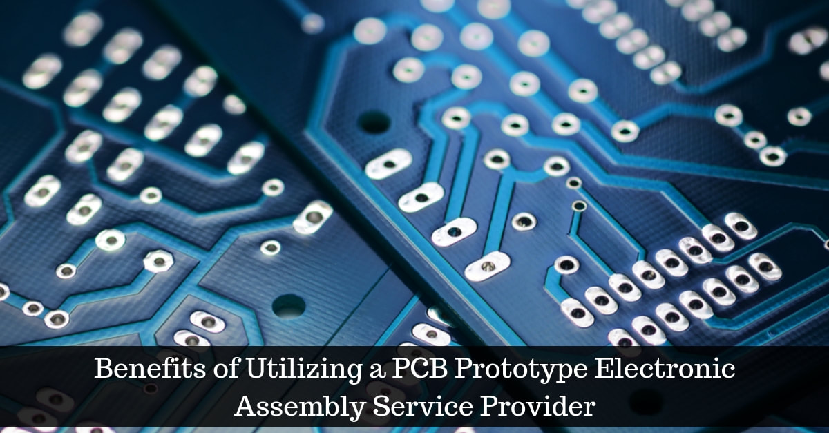 A manufacturer developing a PCB prototype quickly and efficiently is the process of rapid PCB Prototyping. Before taking the PCB Assembly into active production, prototyping allows the manufacturer to examine the Printed Circuit Board Assembly. Through this process, design issues, errors, and malfunctions with the Assembly gets discovered at an initial stage. Thus, till the time final design gets established it allows the manufacturer to make design adjustments.
Rapid PCB Prototyping by its precise nature shortens the life cycle of the product, seizing what used to require weeks to complete and performing a little. This advantage solely makes prototyping a decisive dilemma to traditional PCB assembly services. With an acute degree of assurance where the final design will be the best design possible, allows prototyping in achieving this as there is frequently a rush to market to produce some electronic devices. To examine the needs of your prototype circuit board assembly, there are various benefits of utilizing a prototype electronic assembly specialist firm. In this article, we will discuss a few advantages of working with electronic manufacturing services (EMS) provider company — PCC. Quick-Turn Prototype Services For both turnkey and consigned prototypes, PCC provides reliable electronic prototype development services. Our rapid prototyping services help the client with faster design cycles and production capabilities. By involving us in the early stages of production, clients through these service benefits with lower product development cost and market them faster. Within two business working days, we deliver turnkey PCB assemblies. PCC’s Offerings
PCC apart from PCB Prototyping & NPI Services also offers New Product Introduction (NPI) Service. We provide complete end-to-end NPI service, starting from product analysis, prototyping, testing and confirmation against the specifications, to quality compliance and finally a seamless transition to the production phase. As PCBA Prototyping and NPI build are imperative to speed up “time to market” and successful introduction of new product, it is crucial to partner with a reliable and experienced EMS provider, who ensures successful NPI, which exactly matches the mentioned specifications. PCC with 27+ years of experience in delivering excellent quality, quick turn PCBA prototyping, and NPI services acquire a highly skilled team which is regularly trained by IPC certified trainers. Also, our soundtrack record and consistent performance have earned us the recognition as the best electronic prototype development team in the USA. 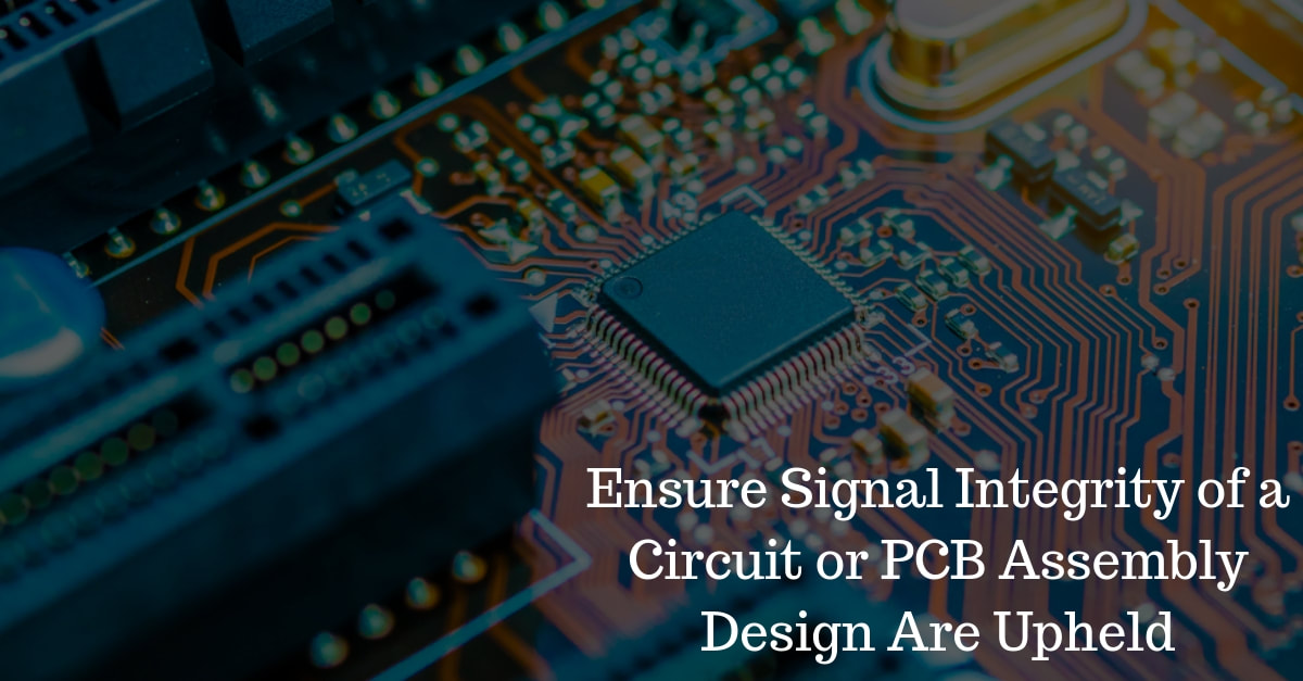 Within the digital circuits rise the use of frequencies causes an effect of the integrity of the signals carried, where comparatively short connections act as cables. In PCB assembly and circuit design, signal integrity has become an increasingly critical element. As applying to the analogue domain modified by effects, signals which considered as purely digital. Also, for any circuit design signal integrity now a significant issue as these effects cause circuits not to work. In today’s high-speed processor designs interpreting the importance of signal integrity, it is essential to incorporate design simulations and check during the Printed Circuit Board design and layout process. Circuit boards effectively need undergoing signal integrity engineering. However, if this is not carried out at the time of design, you need not worry as there is little that can be done once a completed board is built. In view of this the top PCB assembly design software packages incorporate options for including signal integrity engineering. Apart from this, as the design proceeds, it enables checks to be carried out. In this way, to ensure the signal integrity is correctly engineered, PCB layout can be optimized in this manner and minimized once the problem occurring the finished PCB is available for its test. Signal Integrity Issues To ensure that the signal integrity of a printed circuit board or circuit design are maintained, and there are few main areas of circuit design and layout required to take into consideration. Besides, all the issues must address to ensure that signal integrity is maintained and not distorted in any way, also the data is corrupted. In this way, without any errors, the system is able to operate satisfactorily and at the required speed. Impedance Corresponding As the frequencies increase, to the fact that lines on printed circuit boards act more like cables, it is necessary to consider the way in which the impedances need to be matched to ensure good signal integrity. Suppose if there is a mismatch between the line and load, then not all the energy of a waveform is absorbed by the load. As a result, the unabsorbed energy is reflected back along the line. However, there is a mismatch between the transmitter and the line, if it again does not absorb. Thus, it in turns, causes overshoot and ringing linking to poor signal integrity and causing rise to signal errors. Therefore, it is essential to match the cable to the line drivers or transmitters and the line receivers if you want to overcome with this problem. To help in maintaining good levels of signal integrity, there are plenty of ideas that can be implemented. The clocking circuitry is one of the areas to which particular attention should be paid, as it generates a regular clocking pulse that develops a background noise if the signal integrity measures are unincorporated. To ensure that all chips are adequately decoupled enduring another way of improving signal integrity, as poor decoupling will add to the noise present on the circuits. As a result, this may signal integrity. PCC is committed to delivering quality Electronic Manufacturing Services (EMS) and solutions. We also specialize in rapid PCB assembly & system manufacturing services, providing PCB Assembly Services for low and medium volume, high mix products, to varied customer markets globally. From multi-layering to flexible PCBs, PCC has expertise in each aspect of Printed Circuit Board Assembly and manufacturing services. Apart from this we also support simple, small boards to complex HDI boards in volume or prototypes.  To show circuit functionality and be readable PCB assembly layout designers in the past worked from schematics that usually drawn in a meaningful way. For instance, angled wires pointing to each other indicates by the cross-page connection. The PCB designers logically made the physical parts placement follow the schematics, and the components that formed functional groupings tended to remain co-located. Usually, the schematics can be read and understood by others, which includes those schematics that were used later to perform troubleshooting, deduce circuit operation, and repair. However, it was relatively easy to recreate a schema from such a PCB assembly. More then, CAE and CAD came along. Into an electronic Etch A Sketch capture tool the art of schematic drawing became debased, whose primary purpose was to create a netlist. So, to complete the planting of the copper traces the PCB designer could use a "rat's nest" on-screen display. In the digitized dumbing-down, any semblance of analog rules or communication between the design engineer and the PCB layout designer was lost. Based on actual PCB placement and package pin-outs, reverse analysis is a two-pass effort requiring an initial physical schematic. Re-drawing the captured circuits in a logical and comprehensible fashion the series of the functional schematic followed. Moreover, the PCB assemblies’ representation is the real schematic. As on the PCB assembly, components drawn in the same orientation and with GDS or EBC physical pins transistors shown in their representative packages. Arranged in the same way relay switches are sown with their terminals as they appear from the top. With the display of functional names and internal logic elements, ICs drawn in their packages. Relating components to a later functional schematic strongly varies on the physical schema, as most of the times a PCB assembly does not have reference designators in the silkscreen. It is impossible to figure out what is going on electrically. However, the result is a very readable and understandable depiction once this has been re-drawn into a meaningful functional schematic. Temporarily color-coding the nets on the physical drawing make the transfer to the technical drawing less prone to error and when dragged around for readability, flexible wires follow the components. Unfortunately, when an element is rotated or flipped, TinyCAD does not keep wires connected. For instance, you have your physical schematic drawn out on a single page, with everything scrunched up close together, impossible to make any sense of the actual electrical functions and long runs of closely spaced wires. Setting its color to bright purple, width to 25 and apply to the entire net with just a click on a fence, suddenly that net jumps off the page at you. Additionally, any net throughout the page with the same name attached will also brighten into visibility. Hence, an individual should have some form of revision control to keep track of the latest updated drawing when others need access to it. So is your PCB assembly no longer manufactured or you need any replacements or capacity additions? Lost your drawings or schematics from corrupted files? Reverse engineer is the best solution. Reverse engineering of PCB’s is one of PCC specialties and our PCB and PCA knowledge with long years of manufacturing experience, has enabled us to provide optimum PCB Reverse Engineering Services. With proficiency and understanding of PCB Reverse Engineering Process, PCC has a dedicated team of engineers following IPC design specifications and work on simple to the most complex PCB/PCA projects. 
The term ‘system integration’ refers to Box build, which includes all the other assembly work involved in an electromechanical assembly, other than the production of the printed circuit board (PCB). The box build assembly is also an electromechanical assembly process that consists of installation and routing of cabling or wire harnesses, installation of sub-assemblies and components and enclosure fabrication. A large cabinet full of wires or a small enclosure or a complex fully assimilated electromechanical system with pneumatics and electronics, the box build can mean a Printed Circuit Board Assembly (PCBA). The box build assembly process can include varying degrees of complexity at each step and is specific to each project. For instance, merely placing a printed circuit board assembly (PCBA) within an enclosure can be one of its levels. Whereas, the complex task of connecting a PCBA to a user interface display may be a subsequent step. Installation of sub-assemblies, routing of cabling or wire harnesses, installation of other components and fabrication of enclosures comprises the most common box build assembly processes. Let's have a look at the box build assembly services. It consists of:
Few things to keep in mind while considering a box build assembly process Are you considering box build assembly process in near future? If so, then here are few things to keep in mind before considering a box build assembly process. 3D CAD Model There are many CAD packages that offer free drawing viewers. If at all possible then you should provide 3D CAD models, as it aids to visualize the final product. Most of the forward-thinking EMS providers possess CAD packages, enabling easy conversion of drawings into build instructions, as well as updates, if required. Also, a layout drawing with the information of key components should be incorporated. Product Dimensions Exact size and weight of the assembly must include in the product dimensions of the unit. Therefore, this detail information is a must to inform the EMS provider as it is not only beneficial for shipping but also to make decisions about how the units will control throughout the complete box build assembly process. Also, you ought to decide and inform your EMS provider how you need the finished product to be packed and transported. The methods that are influenced by dimension information are packaging, storage, transportation, and shipping. Bill of materials (BOM) For any Electronic Manufacturing Service provider, bill of materials or BOM is one of the most critical pieces of information, which is also known as the formula, recipe, or ingredients list. Bill of materials assists the EMS provider in getting an idea of all the essential components and materials that need to be sourced. A specific purpose, procurement process, and associated cost is included in every item on a bill of materials. It is not necessary to give out only significant piece of information, you can also define the smaller elements such as nuts and bolts, tie wraps, wires, adhesives, washers, heat shrink and much more. Even if these elements considered as consumables, they still have price that you need to pay for buying. Thus, to avoid unexpected cost additions and any unpredicted production delays, a well-crafted bill of material can assist the Electronic Manufacturing Services (EMS) provider. Testing For any electrical devices, safety comes first as it is one of the prime concerns. Therefore, you need to specify the necessary electrical safety testing like earth bonding and flash tests for electrical system of box build assemblies. It is preferable to discuss with your EMS provider if you wish to perform functional testing, factory acceptance testing, visual inspection, and much more as they are skilled and know-how of what works best. Hence, both simple and complex box build assembly depends upon comprehensive requirements gathering and whenever you decide on having a box build assembly process, it is better to keep all this data handy. Also to get the best result, you should discuss it with your EMS provider. So, it is better to be acquainted with all these information and decisions beforehand. PCC-I is one such company that offers sub-system and complete PCB box-build and system assembly services to customers.  Both cable assembly and wire harness play a significant role in connecting electrical and electronic components. To a great extent, these electronic components are distinct from one another although they are used quite interchangeably at times and are frequently used in a similar fashion. It is very significant to identify the difference between wire harness and cable assembly, as it will give you a better perceptive of why the two are so distinct.
Wire Harnesses is small and lightweight The harness consists of a single cord or a group of wire strands covered by an exterior sheath made from thermoplastic or thermoset material that is used as sheathing in cable assemblies. These wire groups are then bound and held together using the tubing, cable tie or woven braiding. In most electronic ignition, the harness is used for connections between starters and other motor starting units, along with connecting the whole vehicles. This wiring installation plays a crucial role in facilitating delivery of power and information across the connection points. An array of crucial roles is severed by using wire harness in vehicles for connecting battery cable, car audio system, ignition system, AC, etc. As these systems play critical job to safeguard car safety and comfort manufacturers take extra precautions to ensure quality. In general, every wire harness passes through several tests before finally being installed. In today’s era, wire harnesses have become extremely important in modern day advanced car models. In order to deliver optimum output and outrageous performance for years, experts in leading wire harness manufacturers predominantly stress on proper configuration of the circuits, efficient design of the harnesses and quality materials. Cable Assembly provides added protection A cable assembly consists of a group of wire cables, covered by an exterior sleeve made of heavy-duty material like vinyl, thermoplastic rubber, or shrink-wrapped thermoplastic. It offers an advantage of having an extra layer of plastic sheathing and protects against elements which helps while working in the dangerous environment. A cable assembly consists of a group of wire cables, covered by an exterior sleeve made of heavy-duty material like vinyl, thermoplastic rubber, or shrink-wrapped thermoplastic. It is also used in various applications. The exterior sleeve in cable assembly that actually protects cables from moisture, heat, friction, dust and wear and tear of uses make them ideal for using outdoor. As far as the quality of cable assembly is concerned, the quality of outer sheath is also a key determinant factor. Within an exterior sheath, cable assemblies bind the wiring cables together which is generally made of a material that can withstand wear and tear of uses in a variety of environments. As a result, cable assemblies are widely preferred for industries and applications where strenuous exposures like compression, heat, moisture, friction and abrasion and other hazards are present. It is due to strong outer sheathing in cable assembly that can protect the inside wires from a whole array of damages and environmental vulnerabilities. Which electronic components are better? Both the electronic components – Cable Assembly and Wire Harness are designed for the different environment, however, they help in keeping cables and wires organized. Cable assemblies are designed as per the size of the area used in and also the environmental factors which they will encounter. As cable assemblies are easier to route around components and equipment, it preferred to wire harnesses. Whereas, wire harnesses are smaller and lighter and can be sourced at a lower cost to manufacturing operations, as lesser labour and material are required. Thus, it is vital for you to know which device you would like to use in your particular application, as both have their own pros and cons. |
 RSS Feed
